cl_hello_world の勉強の続き。
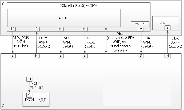
DUTのポートについては、 aws-fpga/hdk/common/shell_v071417d3/design/interfaces/cl_ports.vh に宣言されている。
基本的にこのVerilog Headerを使用することで、どのようなデザインでも使用することができるということか。
cl_ports.vh
   //--------------------------------
   // Globals
   //--------------------------------
   input clk_main_a0,                           //Main clock.  This is the clock for all of the interfaces to the SH
   input clk_extra_a1,                          //Extra clock A1 (phase aligned to "A" clock group)
   input clk_extra_a2,                          //Extra clock A2 (phase aligned to "A" clock group)
   input clk_extra_a3,                          //Extra clock A3 (phase aligned to "A" clock group)
   ...
まず目につくのは、AXIスレーブのレジスタスライスが入っている。
  axi_register_slice_light AXIL_OCL_REG_SLC (
   .aclk          (clk_main_a0),
   .aresetn       (rst_main_n_sync),
   .s_axi_awaddr  (sh_ocl_awaddr),
   .s_axi_awprot   (2'h0),
   .s_axi_awvalid (sh_ocl_awvalid),
   .s_axi_awready (ocl_sh_awready),
   .s_axi_wdata   (sh_ocl_wdata),
   .s_axi_wstrb   (sh_ocl_wstrb),
   .s_axi_wvalid  (sh_ocl_wvalid),
   .s_axi_wready  (ocl_sh_wready),
   .s_axi_bresp   (ocl_sh_bresp),
...
このポートは cl_ports.vh に定義されていた。
cl_ports.vh
   //------------------------------------------------------------------------------------------
   // AXI-L maps to any inbound PCIe access through AppPF BAR0
   // For example, this AXI-L interface can connect to OpenCL Kernels
   // This would connect automatically to the required logic
   // if the CL is created through SDAccel flow
   //------------------------------------------------------------------------------------------
   input sh_ocl_awvalid,
   input[31:0] sh_ocl_awaddr,
   output logic ocl_sh_awready,

   //Write data
   input sh_ocl_wvalid,
   input[31:0] sh_ocl_wdata,
   input[3:0] sh_ocl_wstrb,
   output logic ocl_sh_wready,

   //Write response
   output logic ocl_sh_bvalid,
   output logic[1:0] ocl_sh_bresp,
   input sh_ocl_bready,

   //Read address
   input sh_ocl_arvalid,
   input[31:0] sh_ocl_araddr,
   output logic ocl_sh_arready,

   //Read data/response
   output logic ocl_sh_rvalid,
   output logic[31:0] ocl_sh_rdata,
   output logic[1:0] ocl_sh_rresp,

   input sh_ocl_rready,
何種類かポートが定義されている。この辺は資料を読んでいくと分かってきた。
- PCIe Master Interface from CL
   //-------------------------------------------------------------------------------------------
   // PCIe Master interface from CL
   //
   //    AXI-4 master interface per PCIe interface.  This is for PCIe transactions mastered
   //    from the SH targetting the host (DMA access to host).  Standard AXI-4 interface.
   //-------------------------------------------------------------------------------------------
   output logic[15:0] cl_sh_pcim_awid,
...
- DDR-4 Interface
   //-----------------------------------------------------------------------------------------------
   // DDR-4 Interface
   //
   //    x3 DDR is instantiated in CL.  This is the physical interface (fourth DDR is in SH)
   //    These interfaces must be connected to an instantiated sh_ddr in the CL logic.
   //    Note even if DDR interfaces are not used, sh_ddr must be instantiated and connected
   //    to these interface ports. The sh_ddr block has parameters to control which DDR
   //    controllers are instantiated.  If a DDR controller is not instantiated it will not
   //    take up FPGA resources.
   //-----------------------------------------------------------------------------------------------
- AXI-4 Interface for DDC_C
   //-----------------------------------------------------------------------------------
   // AXI4 Interface for DDR_C
   //    This is the DDR controller that is instantiated in the SH.  CL is the AXI-4
   //    master, and the DDR_C controller in the SH is the slave.
   //-----------------------------------------------------------------------------------
- PCIS AXI-4 interface to master cycles to CL
   input[5:0] sh_cl_dma_pcis_awid,
...
- AXI-L (SDA) MgmtPF, BAR4のアクセスなどに使用される。
   //------------------------------------------------------------------------------------------
   // AXI-L maps to any inbound PCIe access through ManagementPF BAR4 for developer's use
   // If the CL is created through  Xilinx’s SDAccel, then this configuration bus
   // would be connected automatically to SDAccel generic logic (SmartConnect, APM etc)
   //------------------------------------------------------------------------------------------
   input sda_cl_awvalid,
- AXI-L (OCL) AppPF と BAR0 のアクセスなどに使用される。
   //------------------------------------------------------------------------------------------
   // AXI-L maps to any inbound PCIe access through AppPF BAR0
   // For example, this AXI-L interface can connect to OpenCL Kernels
   // This would connect automatically to the required logic
   // if the CL is created through SDAccel flow
   //------------------------------------------------------------------------------------------
   input sh_ocl_awvalid,
- AXI-L (BAR1) AppPF と BAR1 のアクセスなどに使用される。
   //------------------------------------------------------------------------------------------
   // AXI-L maps to any inbound PCIe access through AppPF BAR1
   // For example,
   //------------------------------------------------------------------------------------------
   input sh_bar1_awvalid,
- Debug Bridge
   //-------------------------------------------------------------------------------------------
   // Debug bridge -- This is for Virtual JTAG.   If enabling the CL for
   // Virtual JTAG (chipcope) debug, connect this interface to the debug bridge in the CL
   //-------------------------------------------------------------------------------------------
- Aurora Interface from CL (AXI-S)
   //-------------------------------
   output [NUM_GTY-1:0]        cl_sh_aurora_channel_up,
   input [NUM_GTY-1:0]         gty_refclk_p,
   input [NUM_GTY-1:0]         gty_refclk_n,
- HMC Interface
   //-----------------------------------------------------------------
   // HMC Interface -- this is not currently used
   //-----------------------------------------------------------------
                               /* HMC0 interface */
   output wire                 hmc0_dev_p_rst_n ,
   input wire                  hmc0_rxps ,
...
ソフトウェアサイドからは、これらのインタフェースにアクセスするようなコードを記述する。
aws-fpga/hdk/cl/examples/cl_hello_world/software/runtime/test_hello_world.c
    /* write a value into the mapped address space */
    uint32_t expected = byte_swap(value);
    printf("Writing 0x%08x to HELLO_WORLD register (0x%016lx)\n", value, HELLO_WORLD_REG_ADDR);
    rc = fpga_pci_poke(pci_bar_handle, HELLO_WORLD_REG_ADDR, value);

    fail_on(rc, out, "Unable to write to the fpga !");

    /* read it back and print it out; you should expect the byte order to be
     * reversed (That's what this CL does) */
    rc = fpga_pci_peek(pci_bar_handle, HELLO_WORLD_REG_ADDR, &value);
    fail_on(rc, out, "Unable to read read from the fpga !");
    printf("=====  Entering peek_poke_example =====\n");
    printf("register: 0x%x\n", value);
    if(value == expected) {
        printf("TEST PASSED");
        printf("Resulting value matched expected value 0x%x. It worked!\n", expected);
    }
    else{
        printf("TEST FAILED");
        printf("Resulting value did not match expected value 0x%x. Something didn't work.\n", expected);
    }